RenhotecIC PD fast charge decoy and boost: convert 5V to 12V


PD fast charge decoy and boost: convert 5V to 12V
Sometimes I have to do some small productions at home or help others develop simple products, so I have a lot of chips and tools at home. Some time ago, I made a product for others, and the power supply was 12V, but during debugging, I found that there was no 12V power supply, so I was anxious. I happen to have a decoy and a booster module at hand. Since the power consumption is relatively small, I tried the decoy and booster solutions, and they are relatively easy to use. I will share with you briefly.
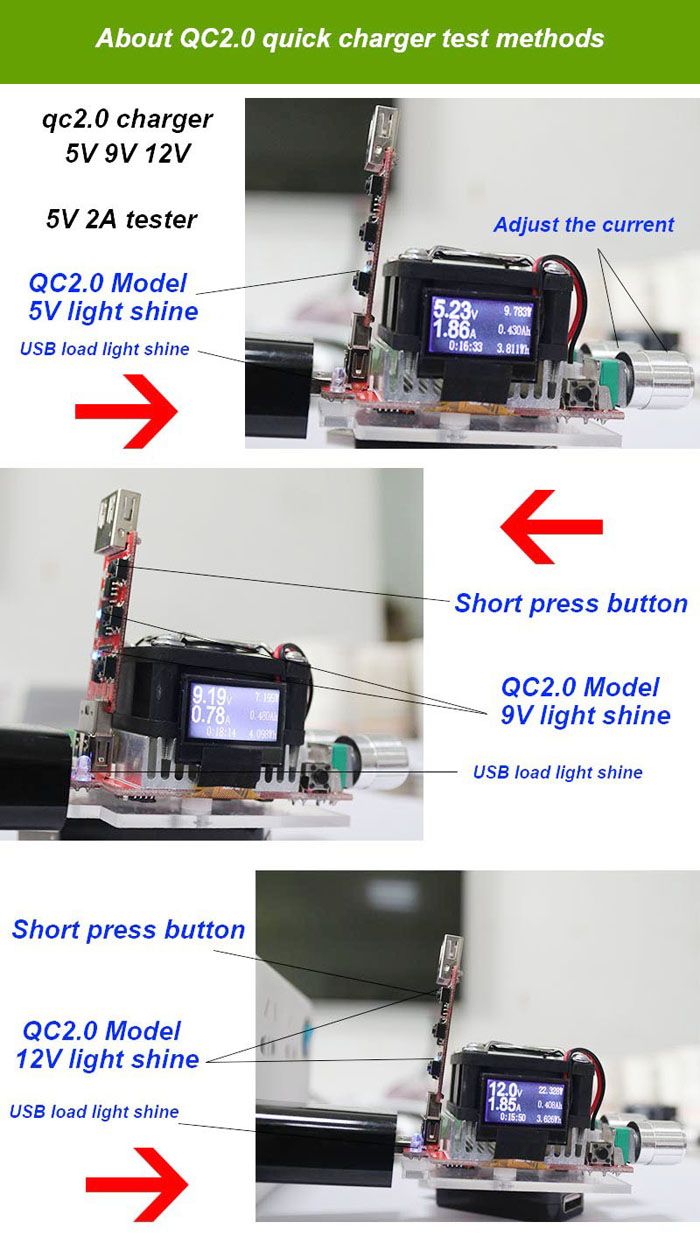
The 5V power supply in my home is changed from an obsolete 5V mobile phone charger. The mobile phone charger has a fast charging function and supports commonly used fast charging protocols, such as PD, QC, etc. When the fast charging protocol is established, it can output 9V Or 12V, otherwise the default output is 5V. At present, the technical solution of mobile phone charger is relatively fixed, consisting of synchronous rectification, PWM controller, high-frequency transformer and fast charging protocol controller, etc. The typical circuit is shown in the figure below.
How do I change the 5V of the phone charger to 12V? Decoys and boost modules are used here.
1 Use PD fast charge decoy device
There are two options for converting 5V to 12V output. If the fast charging protocol is supported, a fast charging decoy can be purchased to make the charger continue to output 12V in the fast charging state, provided that it supports PD fast charging; the second method The way is to choose a boost module. The PD fast charging decoy is shown in the figure below.
It just so happens that I have this thing at home. The function of this thing is to simulate the handshake between the mobile phone and the charger. After the fast charging protocol is matched, the fast charging function can be realized. It happened that there was this decoy on the recommendation page and the price was not expensive. Out of curiosity, I bought a few back. Of course, I took it apart, and inside was a chip with a fast charging protocol stack. 2 with booster module
The boost module in my home is realized by the XL6008 scheme. It was an old urchin's activity. I got only one piece.
The input voltage range of XL6008 is DC(3.6-32)V, and the maximum output is 60V. After stripping the USB cable, find the VBUS and GND lines, and solder VBUS to the positive pole of the input terminal of the boost module; connect GND to the input terminal of the boost module. The negative electrode can be set to output 12V by adjusting the sliding rheostat. The advantage of adopting this scheme is that the charger itself is not damaged, and it is safer and more convenient to use.
I have tried these two solutions. Since the power consumption of the whole board is about 200mA, both solutions can be realized, and no problems were found during the debugging process. Here I would like to share my experience and ideas with you. It is still recommended that you use switching power supply and regulated power supply to debug products, especially in the case of relatively large power consumption. In the process of debugging products, safety comes first.


Leave a Comment